System-on-Modules are used in many applications worldwide. Find out more about the function and benefits of such a module here.
A system-on-module (SoM) is a system unit that combines all the hardware system components that are important for a specific task on a module board (e.g. processor, memory, clock generator, etc.). Appropriate interfaces and connection options are often provided on the board to enable communication with an external environment. Developers can therefore use an SoM as a building block to fulfill the core processing requirements for various task designs with minimal technical effort. For this reason, system-on-modules are predominantly used in so-called “embedded systems”.
System-on-Modules enable a high degree of flexibility in the development process, as they can be easily adapted as required. Advanced technologies (e.g. AI) can also be easily integrated. As developers do not have to deal with the challenges of creating such boards, they can concentrate on developing other, product-specific functions. This saves time and money!
As system-on-modules are tested in advance, the development risk of new systems is reduced many times over. By providing multiple applications on a single board, the overall complexity of a system design is also reduced.
Smart System-on-Modules often also integrate analog and digital functions, which gives them a major advantage for the measurement technology sector. Here, real, physical (i.e. analog) values must be recorded and converted into digital data. As enormous precision is required here, depending on the area of application, the components of such a SoM must be very finely tuned to each other and highly reliable. This is where so-called AD converters (analog-to-digital converters, or ADCs for short) come into play.
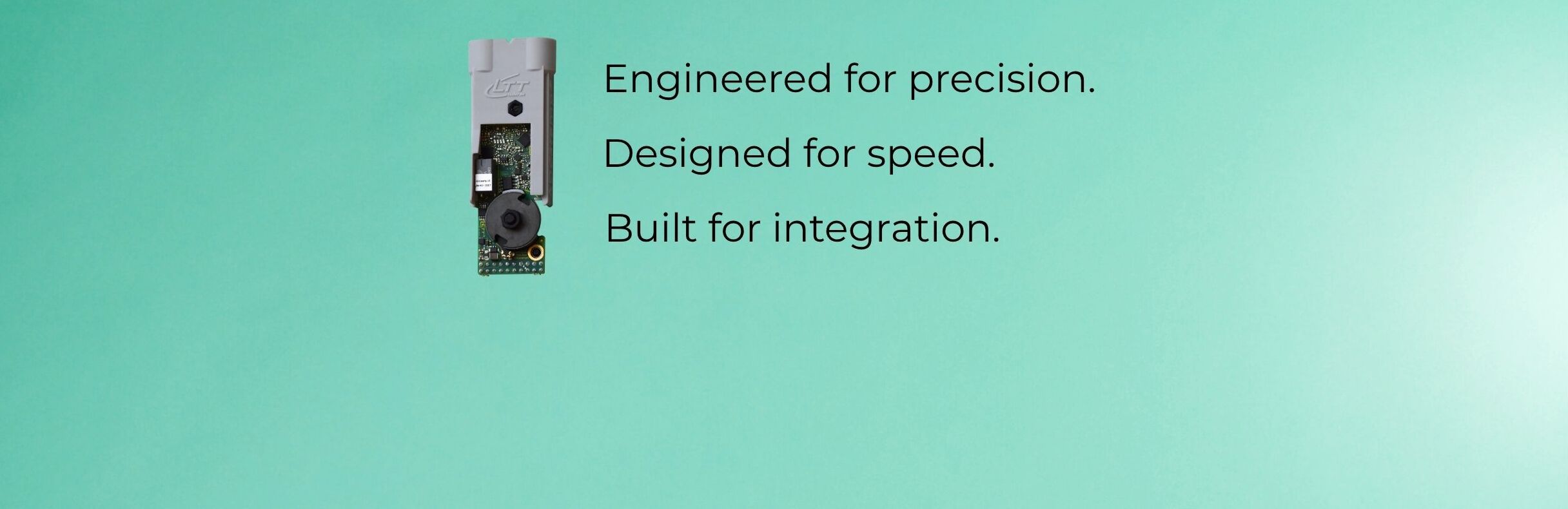
The ADCstamp developed by Labortechnik Tasler has been designed as such an AD-Converter as system-on-module and offers many advantages that enable flexible use with superior measurement technology. The ADCstamp can be integrated into all existing system environments, requiring only a few minutes for commissioning. For hardware developers, this now offers access to our high-precision measurement technology, which we have been successfully marketing for over 25 years in the form of our own measurement devices!
Both high-voltage inputs and sensitive sensor signals can be connected directly to the ADCstamp. The integrated preamplifiers meet the highest demands in terms of noise, distortion, linearity, measurement deviation, temperature drift, gain flatness and crosstalk. The galvanic isolation is designed and tested for 5000V overvoltage peaks.
A huge advantage: developers can focus on other functions and do not have to worry about the challenges of designing a measurement channel themselves. The following diagram shows what such an implementation might look like:
em")
")
Curious? Find out more about the ADCstamp under the following link or contact us directly!
Innovation ADCstamp